Without silicon, our modern daily life would look entirely different. It is found in every microchip but also in baking moulds, lubricants, cosmetics, and plastics: the element silicon.
Silicon – What Is It and Where Does It Occur?
Silicon is a chemical element with the atomic number 14, located in the third period and the 14th position of the periodic table. With four valence electrons, it belongs to group 14, also called the carbon group. Its symbol is Si. It is not to be confused with the term silicone, a family of silicon-based polymers. These silicon-based silicone rubbers are used, among other things, for manufacturing silicone tubing and seals.
In oceans, it exists as dissolved silicic acid. In the plant and animal kingdoms, silicon dioxide (SiO2) can be found in diatoms, sponges, radiolarians, bamboo, and horsetail plants. After oxygen, it is the second most abundant element on Earth.

In everyday life, it is encountered not only as a component of microchips and photovoltaic systems but also in silicone rubbers that are processed into sealants, hoses for coffee machines, cookware, and baking moulds.
Properties of Silicon
The pure element is bluish to dark grey and shiny. It forms a passive silicon dioxide layer on its surface, making it insoluble in water and most acids. Only chlorine-containing acids and hydrofluoric acid can dissolve it. In hot alkaline solutions, silicates are formed.
At very high temperatures, it reacts with carbon to form carbide (SiC), with nitrogen to form silicon nitride (Si3N4), and with sulfur to form silicon disulfide (SiS2). The element crystallises in a so-called diamond lattice, which accounts for its high hardness and brittleness.
Is Silicon a Semiconductor?
In the periodic table, it lies between metals and non-metals and is classified as a metalloid. Its electrical conductivity, at about 5·10-6 S/cm, lies between that of metals (>104 S/cm) and non-metals (<10-8 S/cm). It is, like germanium, an elemental semiconductor; others are compound semiconductors such as gallium arsenide or cadmium selenide, and organic semiconductors.


Silicon offers advantages over other semiconductors because the raw material is inexpensive and widely available, and its surfaces can easily form oxides. This dioxide is an excellent electrical insulator. By introducing foreign atoms – a process known as doping – the conductivity of the element can be precisely controlled.
Purity Grades and their Applications
Silicon is an important base material in metallurgy, photovoltaics, and microelectronics. Depending on the application, different purity levels are required.
For metallurgical applications, a purity of 98–99 % is sufficient; this is referred to as metallurgical grade (abbreviated: Simg). In photovoltaics, silicon with a purity greater than 99.99 % is required (Sisg). For microelectronic applications, only ultra-pure semiconductor silicon is used, with a purity of at least 99.9999999 %. The designation is “electronic grade” (Sieg).
Production of Raw Silicon
The starting material for obtaining the element is silicon dioxide.
The remaining raw silicon can be used as an alloy component or for producing silicones. Further purification steps are required for photovoltaic use.
Production of Solar-Grade Silicon
A common purification method is the trichlorosilane process. In this process, raw silicon is reacted with hydrogen chloride at about 300 °C to form hydrogen and trichlorosilane (SiHCl3), which is then purified by distillation.

The purified trichlorosilane is then reacted with hydrogen at around 1100 °C in a quartz reactor containing heated thin silicon rods. This produces hydrogen chloride, silicon tetrachloride, and elemental silicon, which deposits on the rods. The diameter of these rods can eventually exceed 30 cm.
This process yields polycrystalline material consisting of many irregularly arranged single crystals, suitable for manufacturing solar cells.
Production of Semiconductor-Grade Silicon
For microelectronic applications, coils are placed around pre-purified silicon rods in a vacuum. When high-frequency alternating current is applied, the material melts internally and impurities sink to the bottom. This process is repeated until the required purity is achieved.
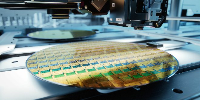
Using the so-called Czochralski process, monocrystalline silicon is produced from polycrystalline material. The polycrystalline feedstock is melted in a quartz crucible under a protective gas atmosphere. Dopants such as boron or phosphorus can be added to the melt. Above the melt, a rotating single crystal — the so-called seed crystal — is positioned so that it touches the surface. Silicon from the melt deposits onto the seed crystal, adopting its crystal structure. The crystal is then slowly pulled upwards at a rate between 2 and 25 cm/h. From these ingots, which can be up to two metres long, thin slices called wafers are cut and further processed into microchips.


Manufacturing microchips is an extremely complex process. Producing microchips on a 300 mm wafer with conductor paths between 28 nm and 32 nm requires around 1500 process steps, taking roughly three months. Modern processors consist of more than one billion transistors and fit on an area smaller than a thumbnail.
Applications in Metallurgy
Raw silicon is an important alloying component in metallurgy. In aluminium casting alloys, it improves casting behaviour as well as corrosion and wear resistance. The alloy silumin consists of about 87 % aluminium and 13 % silicon and is used for manufacturing engine and gearbox housings in the automotive, aerospace, and machinery industries.
In iron alloys, silicon increases scale resistance, tensile strength, and yield strength, and acts as a reducing agent. SiMo alloys, which contain around 2–3 % silicon and aluminium and about 1 % nickel and molybdenum, are special alloys used at temperatures up to 800 °C, for example in turbochargers, exhaust manifolds, and exhaust systems. Ferrosilicon, produced from iron ore and quartz, serves as a master alloy in steel and cast-iron production.
Applications in Photovoltaics
Solar cells are made from both polycrystalline and monocrystalline material.
Polycrystalline solar cells have a light, bluish surface. Monocrystalline cells can be recognised by their uniform dark colour and rounded corners, as they are cut from single-crystal silicon wafers. They are suitable when only limited space is available for power generation.
Raw Silicon as a Base Material for Silicone Rubbers
Raw silicon with a purity of at least 99 % and chloromethane (CH3Cl) serve as feedstock for silicone production. In the so-called Müller–Rochow process, powdered silicon (particle size 50–500 µm) is mixed with copper as a catalyst and activators in a fluidised-bed reactor. Chloromethane is introduced from below and flows through the powder mixture. The reaction occurs at 260–320 °C and pressures between 1 and 5 bar.
This reaction yields a mixture of chloromethylsilanes, which are separated by fractional distillation. The most important compound for silicone production is dimethyldichlorosilane ((CH3)2Cl2Si). During hydrolysis, hydrogen chloride is released, and the chlorine atoms are replaced by hydroxyl groups (–OH). Through subsequent polycondensation, water molecules are eliminated and polydimethylsiloxane is formed. These polysiloxanes can be further crosslinked or functionalised in additional reactions.
Silicones are components of silicone oils, resins, and rubbers. Silicone oils consist of linear polysiloxane chains and are used as lubricants, antifoaming agents, sealants, and hydraulic fluids.


Silicone rubbers consist of long-chain, three-dimensionally crosslinked polysiloxanes. They are used as sealing materials and electrical insulators. Implants, baby bottle teats, and baking or ice-cube moulds are made from physiologically safe silicone grades. Furthermore, silicone rubbers are processed into pump tubing, medical tubing, semi-finished products, plugs, and seals such as O-rings.
Compared with other rubber hoses, silicone hoses offer an exceptionally wide operating temperature range from −60 °C to +300 °C. Even at low temperatures, they remain flexible and elastic. Silicone hoses are physiologically harmless and suitable for use in the food and medical industries.
Silicone resins are even more highly crosslinked than silicone rubbers. They serve as insulating, heat- and weather-resistant coatings, lacquers, moulding compounds, and laminates.
Silicon on the Moon
In 1969, the crew of Apollo 11 left a silicon wafer the size of a 50-cent coin on the Moon, enclosed in an aluminium case inscribed “From Planet Earth – July 1969”. On the wafer itself were goodwill messages from 73 world leaders, including US presidents Richard M. Nixon, Lyndon B. Johnson, and John F. Kennedy. Each message was photographed and miniaturised to a size much smaller than a pinhead – a microscope would be required to read them.

Due to the increasing importance of electronic components, the term Silicon Age was coined. Likewise, the high-tech region in California known as Silicon Valley underscores the element’s fundamental role in the semiconductor industry.
Image Sources:
Featured image: © SweetBunFactory – stock.adobe.com
Amorphous silicon dioxide: LHcheM, CC BY-SA 3.0 <https://creativecommons.org/licenses/by-sa/3.0>, via Wikimedia Commons
Monocrystalline solar modules: © visdia – stock.adobe.com
Silicon wafer from Apollo 11 mission: © NASA, Public domain, via Wikimedia Commons